|
High-throughput three-dimensional lithographic microfabrication
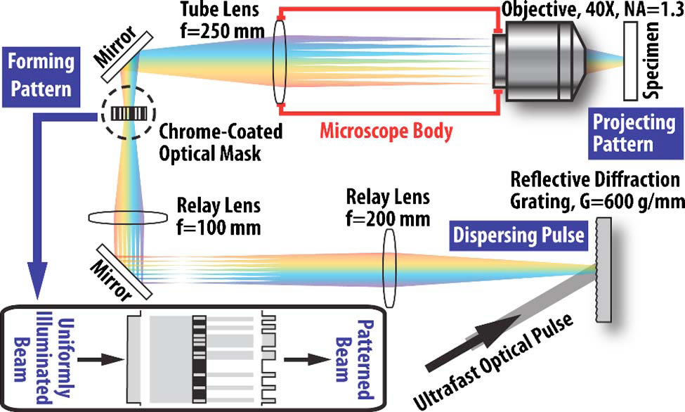
SMART & MIT researchers have developed a 3D lithographic microfabrication process that is high throughput, scalable, and capable of producing arbitrary patterns. It offers the possibility for industrial scale manufacturing of 3D microdevices such as photonic crystals, tissue engineering scaffolds, and microfluidics chips. This method is based on depth-resolved wide-field illumination by temporally focusing femtosecond light pulses. Characterization of the axial resolution of this technique has been performed, and the result is consistent with the theoretical prediction. As proof-of-concept experiments, they have demonstrated photobleaching of 3D resolved patterns in a fluorescent medium and fabricated 3D microstructures with SU-8 photoresist.The details have been published in May 15, 2010 issue of OPTICS LETTERS (Daekeun Kim and Peter T. C. So, Optics Letters, Vol. 35, pp. 1602-1604).

Schematic diagram of 3D lithographic microfabrication system. Inset, how planar pattern
is created through the optical mask.
|
 |